- 您现在的位置:买卖IC网 > Sheet目录1214 > EVAL-ADE7880EBZ (Analog Devices Inc)BOARD EVAL FOR ADE7880
�� �
�
�ADE7880�
�I� 2� C� Read� Operation� of� Harmonic� Calculations� Registers�
�The� registers� containing� the� harmonic� calculation� results� are�
�located� starting� at� Address� 0xE880� and� are� all� 32-bit� width.�
���registers� at� a� time� in� a� burst� mode.� This� burst� mode� is�
�accomplished� in� two� stages.� As� seen� in� Figure� 102,� the� first�
�stage� sets� the� pointer� to� the� address� of� the� register� and� is�
�identical� to� the� first� stage� executed� when� only� one� register� is�
�read.� The� second� stage� reads� the� content� of� the� registers.� The�
�second� stage� begins� with� the� master� generating� a� new� start�
�condition� followed� by� an� address� byte� equal� to� the� address� byte�
�used� when� one� single� register� is� read,� 0x71.� After� this� byte� is�
�received,� the� ADE7880� generates� an� acknowledge.� Then,� the�
�ADE7880� sends� the� value� of� the� first� register� located� at� the�
�Data� Sheet�
�connection� between� the� ADE7880� SPI� and� a� master� device�
�containing� an� SPI� interface.�
�The� SS� logic� input� is� the� chip� select� input.� This� input� is� used�
�when� multiple� devices� share� the� serial� bus.� Drive� the� SS� input�
�low� for� the� entire� data� transfer� operation.� Bringing� SS� high�
�during� a� data� transfer� operation� aborts� the� transfer� and� places�
�the� serial� bus� in� a� high� impedance� state.� A� new� transfer� can�
�then� be� initiated� by� returning� the� SS� logic� input� to� low.�
�However,� because� aborting� a� data� transfer� before� completion�
�leaves� the� accessed� register� in� a� state� that� cannot� be� guaranteed,�
�every� time� a� register� is� written,� its� value� should� be� verified� by�
�reading� it� back.� The� protocol� is� similar� to� the� protocol� used� in�
�I� 2� C� interface.�
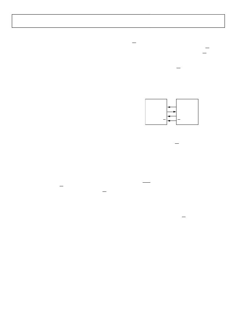
�ADE7880� SPI� DEVICE�
�pointer,� and� after� every� eight� bits� are� received,� the� master�
�generates� an� acknowledge.� All� the� bytes� are� sent� with� the� most�
�significant� bit� first.� After� the� bytes� of� the� first� register� are� sent,� if�
�the� master� acknowledges� the� last� byte,� the� ADE7880� increments�
�MOSI�
�MISO�
�SCLK�
�SS�
�MOSI�
�MISO�
�SCK�
�SS�
�the� pointer� by� one� location� to� position� it� at� the� next� register� and�
�begins� to� send� it� out� byte� by� byte,� most� significant� bit� first.� If� the�
�master� acknowledges� the� last� byte,� the� ADE7880� increments� the�
�pointer� again� and� begins� to� send� data� from� the� next� register.�
�The� process� continues� until� the� master� ceases� to� generate� an�
�acknowledge� at� the� last� byte� of� the� register� and� then� generates� a�
�stop� condition.� It� is� recommended� to� not� allow� locations� greater�
�then� 0xE89F,� the� last� location� of� the� harmonic� calculations�
�registers.�
�SPI-Compatible� Interface�
�The� SPI� of� the� ADE7880� is� always� a� slave� of� the� communication�
�and� consists� of� four� pins� (with� dual� functions):� SCLK/SCL,�
�MOSI/SDA,� MISO/HSD,� and� SS/HSA.� The� functions� used� in�
�the� SPI-compatible� interface� are� SCLK,� MOSI,� MISO,� and� SS.�
�The� serial� clock� for� a� data� transfer� is� applied� at� the� SCLK� logic�
�input.� All� data� transfer� operations� synchronize� to� the� serial�
�clock.� Data� shifts� into� the� ADE7880� at� the� MOSI� logic� input�
�on� the� falling� edge� of� SCLK� and� the� ADE7880 samples it on�
�the� rising� edge� of� SCLK.� Data� shifts� out� of� the� ADE7880� at�
�the� MISO� logic� output� on� a� falling� edge� of� SCLK� and� can� be�
�sampled� by� the� master� device� on� the� raising� edge� of� SCLK.� The�
�most� significant� bit� of� the� word� is� shifted� in� and� out� first.� The�
�Figure� 103.� Connecting� ADE7880� SPI� with� an� SPI� Device�
�SPI� Read� Operation�
�The� read� operation� using� the� SPI� interface� of� the� ADE7880�
�initiate� when� the� master� sets� the� SS/HSA� pin� low� and� begins�
�sending� one� byte,� representing� the� address� of� the� ADE7880� ,� on�
�the� MOSI� line.� The� master� sets� data� on� the� MOSI� line� starting�
�with� the� first� high-to-low� transition� of� SCLK.� The� SPI� of� the�
�ADE7880� samples� data� on� the� low-to-high� transitions� of� SCLK.�
�The� most� significant� seven� bits� of� the� address� byte� can� have� any�
�value,� but� as� a� good� programming� practice,� they� should� be�
�different� from� 0111000b,� the� seven� bits� used� in� the� I� 2� C� protocol.�
�Bit� 0� (read/� write)� of� the� address� byte� must� be� 1� for� a� read�
�operation.� Next,� the� master� sends� the� 16-bit� address� of� the�
�register� that� is� read.� After� the� ADE7880� receives� the� last� bit� of�
�address� of� the� register� on� a� low-to-high� transition� of� SCLK,� it�
�begins� to� transmit� its� contents� on� the� MISO� line� when� the� next�
�SCLK� high-to-low� transition� occurs;� thus,� the� master� can�
�sample� the� data� on� a� low-to-high� SCLK� transition.� After� the�
�master� receives� the� last� bit,� it� sets� the� SS� and� SCLK� lines� high�
�and� the� communication� ends.� The� data� lines,� MOSI� and� MISO,�
�go� into� a� high� impedance� state.� See� Figure� 104� for� details� of� the�
�SPI� read� operation.�
�maximum� serial� clock� frequency� supported� by� this� interface�
�is� 2.5� MHz.� MISO� stays� in� high� impedance� when� no� data� is�
�transmitted� from� the� ADE7880� .� See� Figure� 103� for� details� of� the�
�Rev.� A� |� Page� 76� of� 104�
�发布紧急采购,3分钟左右您将得到回复。
相关PDF资料
EVAL-ADE7953EBZ
BOARD EVAL FOR ADE7953
EVAL-ADF4002EBZ1
BOARD EVAL FOR ADF4002
EVAL-ADG788EBZ
BOARD EVALUATION FOR ADG788
EVAL-ADM1021AEB
BOARD EVAL FOR ADM1021
EVAL-ADM1023EB
BOARD EVAL FOR ADM1023
EVAL-ADM1031EB
BOARD EVAL FOR ADM1031
EVAL-ADM1062TQEBZ
BOARD EVALUATION FOR ADM1062TQ
EVAL-ADM1075CEBZ
BOARD EVAL FOR ADM1075
相关代理商/技术参数
EVAL-ADE7880EBZ
制造商:Analog Devices 功能描述:ADE7880, ENERGY METER, 3 PH, SPI, I2C, E
EVAL-ADE7913EBZ
制造商:AD 制造商全称:Analog Devices 功能描述:3-Channel, Isolated, Sigma-Delta ADC with SPI
EVAL-ADE7953EBZ
功能描述:BOARD EVAL FOR ADE7953 RoHS:是 类别:编程器,开发系统 >> 评估演示板和套件 系列:- 标准包装:1 系列:PSoC® 主要目的:电源管理,热管理 嵌入式:- 已用 IC / 零件:- 主要属性:- 次要属性:- 已供物品:板,CD,电源
EVAL-ADF4001EBZ2
制造商:Analog Devices 功能描述:Evaluation Board For Pll Frequency Synthesizer 制造商:Analog Devices 功能描述:ADF4001 PLL SYNTHESIZER EVAL BOARD
EVAL-ADF4002EB1
制造商:Analog Devices 功能描述:EVAL BOARD - Bulk
EVAL-ADF4002EBZ1
功能描述:BOARD EVAL FOR ADF4002 RoHS:是 类别:编程器,开发系统 >> 评估演示板和套件 系列:- 产品培训模块:Obsolescence Mitigation Program 标准包装:1 系列:- 主要目的:电源管理,电池充电器 嵌入式:否 已用 IC / 零件:MAX8903A 主要属性:1 芯锂离子电池 次要属性:状态 LED 已供物品:板
EVAL-ADF4007EBZ1
功能描述:BOARD EVALUATION FOR ADF4007EB1 RoHS:是 类别:编程器,开发系统 >> 评估演示板和套件 系列:- 标准包装:1 系列:PSoC® 主要目的:电源管理,热管理 嵌入式:- 已用 IC / 零件:- 主要属性:- 次要属性:- 已供物品:板,CD,电源
EVAL-ADF4106EB1
制造商:Analog Devices 功能描述:PLL, Frequency Synthesizer